(Printed circuit board)Electronic circuit board
A
printed circuit board, or
PCB, is used to mechanically support and electrically connect
electronic components using
conductive pathways, tracks or signal traces
etched from copper sheets
laminated onto a non-conductive
substrate. It is also referred to as
printed wiring board (
PWB) or
etched wiring board. A PCB populated with electronic components is a
printed circuit assembly (
PCA), also known as a
printed circuit board assembly (
PCBA).
PCBs are inexpensive, and can be highly reliable. They require much more layout effort and higher initial cost than either
wire-wrapped or
point-to-point constructed circuits, but are much cheaper and faster for high-volume production. Much of the electronics industry's PCB design, assembly, and quality control needs are set by standards that are published by the
IPC organization.
History
The inventor of the printed circuit was the
Austrian engineer
Paul Eisler (1907–1995) who, while working in England, made one circa
1936 as part of a
radio set. Around
1943 the USA began to use the technology on a large scale to make rugged radios for use in
World War II. After the war, in
1948, the USA released the invention for commercial use. Printed circuits did not become commonplace in consumer electronics until the mid-1950s, after the
Auto-Sembly process was developed by the
United States Army.
Before printed circuits (and for a while after their invention),
point-to-point construction was used. For prototypes, or small production runs,
wire wrap or
turret board can be more efficient. Predating the printed circuit invention, and similar in spirit, was
John Sargrove's 1936-1947 Electronic Circuit Making Equipment (ECME) which sprayed metal onto a
Bakelite plastic board. The ECME could produce 3 radios per minute.
During World War II, the development of the anti-aircraft
proximity fuse required an electronic circuit that could withstand being fired from a gun, and could be produced in quantity. The Centralab Division of Globe Union submitted a proposal which met the requirements: a ceramic plate would be
screenprinted with metallic paint for conductors and carbon material for
resistors, with ceramic disc capacitors and subminiature vacuum tubes soldered in place.
[1]
Originally, every electronic component had wire leads, and the PCB had holes drilled for each wire of each component. The components' leads were then passed through the holes and
soldered to the PCB trace. This method of assembly is called
through-hole construction. In 1949, Moe Abramson and Stanislaus F. Danko of the
United States Army Signal Corps developed the Auto-Sembly process in which component leads were inserted into a copper foil interconnection pattern and
dip soldered. With the development of board lamination and etching techniques, this concept evolved into the standard printed circuit board fabrication process in use today. Soldering could be done automatically by passing the board over a ripple, or wave, of molten solder in a
wave-soldering machine. However, the wires and holes are wasteful since drilling holes is expensive and the protruding wires are merely cut off.
In recent years, the use of
surface mount parts has gained popularity as the demand for smaller electronics packaging and greater functionality has grown.
Manufacturing
Materials
Conducting layers are typically made of thin copper foil. Insulating layers
dielectric are typically laminated together with
epoxy resin prepreg. The board is typically coated with a solder mask that is green in color. Other colors that are normally available are blue and red. There are quite a few different dielectrics that can be chosen to provide different insulating values depending on the requirements of the circuit. Some of these dielectrics are
polytetrafluoroethylene (Teflon), FR-4, FR-1, CEM-1 or CEM-3. Well known prepreg materials used in the PCB industry are
FR-2 (Phenolic cotton paper), FR-3 (Cotton paper and epoxy),
FR-4 (Woven glass and epoxy), FR-5 (Woven glass and epoxy), FR-6 (Matte glass and polyester), G-10 (Woven glass and epoxy), CEM-1 (Cotton paper and epoxy), CEM-2 (Cotton paper and epoxy), CEM-3 (Woven glass and epoxy), CEM-4 (Woven glass and epoxy), CEM-5 (Woven glass and polyester). Thermal expansion is an important consideration especially with BGA and naked die technologies, and glass fiber offers the best dimensional stability.
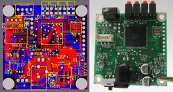
A PCB as a design on a computer (left) and realized as a board assembly populated with components (right). The board is double sided, with through-hole plating, green solder resist, and white silkscreen printing. Both surface mount and through-hole components have been used.
FR-4 is by far the most common material used today. The board with copper on it is called "copper-clad laminate".
In the US, copper foil thickness is specified in units of ounces per square foot (oz/ft
2). One
ounce copper foil has a weight of one oz/ft
2. This works out to a thickness of 0.001344" (1.344 mils) or 0.0341mm. Some PCB manufacturers refer to one ounce copper foil as having a thickness of 35
μm (or simply 35μ) or sometimes 35
micron (or microns or mic.). Two ounce would be 70μ and half ounce would be 17.5μ or thereabouts.
Typical density of a raw PCB (an average amount of traces, holes, and vias, with no components) is 2.15g / cm
3.
Patterning (etching)
The vast majority of printed circuit boards are made by bonding a layer of copper over the entire substrate, sometimes on both sides, (creating a "blank PCB") then removing unwanted copper after applying a temporary mask (e.g. by etching), leaving only the desired copper traces. A few PCBs are made by
adding traces to the bare substrate (or a substrate with a very thin layer of copper) usually by a complex process of multiple
electroplating steps. The PCB manufacturing method primarily depends on whether it is for production volume or sample/prototype quantities.
Commercial (production quantities, usually PTH)
- silk screen printing -the main commercial method.
- Photographic methods. Used when fine linewidths are required.
Hobbyist/prototype (small quantities, usually not PTH)
- Laser-printed resist: Laser-print onto paper (or wax paper), heat-transfer with a household clothes iron onto bare laminate, then etch.
- Print onto transparent film and use as photomask along with photo-sensitized boards. (i.e. pre-sensitized boards), Then etch. (Alternatively, use a film photoplotter).
- Laser resist ablation: Spray black paint onto copper clad laminate, place into CNC laser plotter. The laser raster-scans the PCB and ablates (vaporizes) the paint where no resist is wanted. Etch. (Note: laser copper ablation is rarely used and is considered experimental.)
- Use a CNC-mill with a spade-shaped (i.e. 45-degree) cutter or miniature end-mill to route away the undesired copper, leaving only the traces.
There are three common "subtractive" methods (methods that remove copper) used for the production of printed circuit boards:
- Silk screen printing uses etch-resistant inks to protect the copper foil. Subsequent etching removes the unwanted copper. Alternatively, the ink may be conductive, printed on a blank (non-conductive) board. The latter technique is also used in the manufacture of hybrid circuits.
- Photoengraving uses a photomask and chemical etching to remove the copper foil from the substrate. The photomask is usually prepared with a photoplotter from data produced by a technician using CAM, or computer-aided manufacturing software. Laser-printed transparencies are typically employed for phototools; however, direct laser imaging techniques are being employed to replace phototools for high-resolution requirements.
- PCB milling uses a two or three-axis mechanical milling system to mill away the copper foil from the substrate. A PCB milling machine (referred to as a 'PCB Prototyper') operates in a similar way to a plotter, receiving commands from the host software that control the position of the milling head in the x, y, and (if relevant) z axis. Data to drive the Prototyper is extracted from files generated in PCB design software and stored in HPGL or Gerber file format.
"Additive" processes also exist. The most common is the "semi-additive" process. In this version, the unpatterned board has a thin layer of copper already on it. A reverse mask is then applied. (Unlike a subtractive process mask, this mask exposes those parts of the substrate that will eventually become the traces.) Additional copper is then plated onto the board in the unmasked areas; copper may be plated to any desired weight. Tin-lead or other surface platings are then applied. The mask is stripped away and a brief etching step removes the now-exposed original copper laminate from the board, isolating the individual traces. Some boards with plated thru holes but still single sided were made with a process like this.
General Electric made consumer radio sets in the late 1960s using boards like these.
The additive process is commonly used for multi-layer boards as it facilitates the
plating-through of the holes (to produce conductive
vias) in the circuit board.
PCB copper electroplating machine for adding copper to the in-process PCB | PCB's in process of adding copper via electroplating |
The dimensions of the copper conductors of the printed circuit board is related to the amount of current the conductor must carry. Each trace consists of a flat, narrow part of the
copper foil that remains after etching. Signal traces are usually narrower than power or ground traces because their current carrying requirements are usually much less. In a multi-layer board one entire layer may be mostly solid copper to act as a
ground plane for shielding and power return. For printed circuit boards that contain
microwave circuits,
transmission lines can be laid out in the form of
stripline and
microstrip with carefully-controlled dimensions to assure a consistent
impedance. In radio-frequency circuits the
inductance and
capacitance of the printed circuit board conductors can be used as a delibrate part of the circuit design, obviating the need for additional discrete components.
Etching
Chemical etching is done with ferric chloride, ammonium persulfate, or sometimes hydrochloric acid. For PTH (plated-through holes), additional steps of electroless deposition are done after the holes are drilled, then copper is electroplated to build up the thickness, the boards are screened, and plated with tin/lead. The tin/lead becomes the resist leaving the bare copper to be etched away.
Lamination
Some PCBs have trace layers inside the PCB and are called
multi-layer PCBs. These are formed by bonding together separately etched thin boards.
Drilling
Holes through a PCB are typically drilled with tiny drill bits made of solid
tungsten carbide. The drilling is performed by
automated drilling machines with placement controlled by a
drill tape or
drill file. These computer-generated files are also called
numerically controlled drill (NCD) files or "
Excellon files". The drill file describes the location and size of each drilled hole. These holes are often filled with annular rings (hollow rivets) to create
vias. Vias allow the electrical and thermal connection of conductors on opposite sides of the PCB.
Most common laminate is epoxy filled fiberglass. Drill bit wear is partly due to embedded glass, which is harder than steel. High drill speed necessary for cost effective drilling of hundreds of holes per board causes very high temperatures at the drill bit tip, and high temperatures (400-700 degrees) soften steel and decompose (oxidize) laminate filler. Copper is softer than epoxy and interior conductors may suffer damage during drilling.
When very small vias are required, drilling with mechanical bits is costly because of high rates of wear and breakage. In this case, the vias may be evaporated by
lasers. Laser-drilled vias typically have an inferior surface finish inside the hole. These holes are called
micro vias.
It is also possible with
controlled-depth drilling, laser drilling, or by pre-drilling the individual sheets of the PCB before lamination, to produce holes that connect only some of the copper layers, rather than passing through the entire board. These holes are called
blind vias when they connect an internal copper layer to an outer layer, or
buried vias when they connect two or more internal copper layers and no outer layers.
The walls of the holes, for boards with 2 or more layers, are made conductive then plated with copper to form
plated-through holes that electrically connect the conducting layers of the PCB. For multilayer boards, those with 4 layers or more, drilling typically produces a
smear of the high temperature decomposition products of bonding agent in the laminate system. Before the holes can be plated through, this
smear must be removed by a chemical
de-smear process, or by
plasma-etch. Removing (etching back) the smear also reveals the interior conductors as well.
Exposed conductor plating and coating
PCBs
[2] are plated with solder, tin, or gold over nickel as a resist for
etching away the unneeded underlying copper.
[3] Matte solder is usually fused to provide a better bonding surface or stripped to bare copper. Treatments, such as benzimidazolethiol, prevent surface oxidation of bare copper. The places to which components will be mounted are typically plated, because untreated bare copper oxidizes quickly, and therefore is not readily solderable. Traditionally, any exposed copper was coated with
solder by hot air solder levelling (
HASL). This solder was a
tin-
lead alloy, however new solder compounds are now used to achieve compliance with the
RoHS directive in the
EU and US, which restricts the use of lead. One of these lead-free compounds is SN100CL, made up of 99.3% tin, 0.7% copper, 0.05% nickel, and a nominal of 60ppm germanium.
It is important to use solder compatible with both the PCB and the parts used. An example is Ball Grid Array (BGA) using tin-lead solder balls for connections losing their balls on bare copper traces or using lead-free solder paste.
Other platings used are OSP (organic surface protectant), immersion silver (
IAg), immersion tin, electroless nickel with immersion gold coating (
ENIG), and direct gold (over nickel).
Edge connectors, placed along one edge of some boards, are often nickel plated then
gold plated. Another coating consideration is rapid diffusion of coating metal into Tin solder. Tin forms intermetallics such as Cu
5Sn
6 and Ag
3Cu that dissolve into the Tin liquidus or solidus(@50C), stripping surface coating and/or leaving voids.
Electrochemical migration (ECM) is the growth of conductive metal filaments on or in a printed circuit board (PCB) under the influence of a DC voltage bias.
[4][5] Silver, zinc, and aluminum are known to grow whiskers under the influence of an electric field. Silver also grows conducting surface paths in the presence of halide and other ions, making it a poor choice for electronics use. Tin will grow "whiskers" due to tension in the plated surface. Tin-Lead or Solder plating also grows whiskers, only reduced by the percentage Tin replaced. Reflow to melt solder or tin plate to relieve surface stress lowers whisker incidence. Another coating issue is
tin pest, the transformation of tin to a powdery allotrope at low temperature.
[6]
Solder resist
Areas that should not be soldered may be covered with a polymer
solder resist (
solder mask) coating. The solder resist prevents solder from bridging between conductors and creating short circuits. Solder resist also provides some protection from the environment. Solder resist is typically 20-30 microns thick.
Screen printing
Line art and text may be printed onto the outer surfaces of a PCB by
screen printing. When space permits, the screen print text can indicate
component designators, switch setting requirements, test points, and other features helpful in assembling, testing, and servicing the circuit board.
Screen print is also known as the
silk screen, or, in one sided PCBs, the
red print.
Lately some digital printing solutions have been developed to substitute the traditional screen printing process. This technology allows printing variable data onto the PCB, including serialization and barcode information for traceability purposes.
Test
Unpopulated boards may be subjected to a
bare-board test where each circuit connection (as defined in a
netlist) is verified as correct on the finished board. For high-volume production, a
Bed of nails tester, a fixture or a
Rigid needle adapter is used to make contact with copper lands or holes on one or both sides of the board to facilitate testing. A computer will
instruct the electrical test unit to apply a small voltage to each contact point on the bed-of-nails as required, and verify that such voltage appears at other appropriate contact points. A "short" on a board would be a connection where there should not be one; an "open" is between two points that should be connected but are not. For small- or medium-volume boards,
flying probe and
flying-grid testers use moving test heads to make contact with the copper/silver/gold/solder lands or holes to verify the electrical connectivity of the board under test.
Printed circuit assembly
After the printed circuit board (PCB) is completed, electronic components must be attached to form a functional
printed circuit assembly,
[7][8] or PCA (sometimes called a "printed circuit board assembly" PCBA). In
through-hole construction, component leads are inserted in holes. In
surface-mount construction, the components are placed on
pads or
lands on the outer surfaces of the PCB. In both kinds of construction, component leads are electrically and mechanically fixed to the board with a molten metal solder.
There are a variety of
soldering techniques used to attach components to a PCB. High volume production is usually done with
machine placement and bulk wave soldering or reflow ovens, but skilled technicians are able to solder very tiny parts (for instance 0201 packages which are 0.02 in. by 0.01 in.)
[9] by hand under a
microscope, using tweezers and a fine tip
soldering iron for small volume prototypes. Some parts are impossible to solder by hand, such as
ball grid array (BGA) packages.
Often, through-hole and surface-mount construction must be combined in a single assembly because some required components are available only in surface-mount packages, while others are available only in through-hole packages. Another reason to use both methods is that through-hole mounting can provide needed strength for components likely to endure physical stress, while components that are expected to go untouched will take up less space using surface-mount techniques.
After the board has been populated it may be tested in a variety of ways:
- While the power is on, in-circuit test, where physical measurements (i.e. voltage, frequency) can be done.
- While the power is on, functional test, just checking if the PCB does what it had been designed for.
To facilitate these tests, PCBs may be designed with extra pads to make temporary connections. Sometimes these pads must be isolated with resistors. The in-circuit test may also exercise
boundary scan test features of some components. In-circuit test systems may also be used to program nonvolatile memory components on the board.
In boundary scan testing, test circuits integrated into various ICs on the board form temporary connections between the PCB traces to test that the ICs are mounted correctly. Boundary scan testing requires that all the ICs to be tested use a standard test configuration procedure, the most common one being the Joint Test Action Group (
JTAG) standard.
When boards fail the test, technicians may
desolder and replace failed components, a task known as
rework.
Protection and packaging
PCBs intended for extreme environments often have a
conformal coating, which is applied by dipping or spraying after the components have been soldered. The coat prevents corrosion and leakage currents or shorting due to condensation. The earliest conformal coats were
wax; modern conformal coats are usually dips of dilute solutions of silicone rubber, polyurethane, acrylic, or epoxy. Another technique for applying a conformal coating is for plastic to be
sputtered onto the PCB in a vacuum chamber. The chief disadvantage of conformal coatings is that servicing of the board is rendered extremely difficult.
[10]
Many assembled PCBs are
static sensitive, and therefore must be placed in
antistatic bags during transport. When handling these boards, the user must be
grounded (earthed). Improper handling techniques might transmit an accumulated static charge through the board, damaging or destroying components. Even bare boards are sometimes static sensitive. Traces have become so fine that it's quite possible to blow an etch off the board (or change its characteristics) with a static charge. This is especially true on non-traditional PCBs such as
MCMs and
microwave PCBs.
Design
- Schematic capture or schematic entry is done through an EDA tool.
- Card dimensions and template are decided based on required circuitry and case of the PCB. Determine the fixed components and heat sinks if required.
- Deciding stack layers of the PCB. 4 to 12 layers or more depending on design complexity. Ground plane and Power plane are decided. Signal planes where signals are routed are in top layer as well as internal layers.[11]
- Line impedance determination using dielectric layer thickness, routing copper thickness and trace-width. Trace separation also taken into account in case of differential signals. Microstrip, stripline or dual stripline can be used to route signals.
- Placement of the components. Thermal considerations and geometry are taken into account. Vias and lands are marked.
- Routing the signal trace. For optimal EMI performance high frequency signals are routed in internal layers between power or ground planes as power plane behaves as ground for AC.
- Gerber File generation for manufacturing.
Safety certification (US)
Safety Standard UL 796 covers component safety requirements for printed wiring boards for use as components in devices or appliances. Testing analyzes characteristics such as flammability, maximum
operating temperature, electrical tracking, heat deflection, and direct support of live electrical parts.
The boards may use organic or inorganic base materials in a single or multilayer, rigid or flexible form. Circuitry construction may include etched, die stamped, precut, flush press, additive, and plated conductor techniques. Printed-component parts may be used.
The suitability of the pattern parameters, temperature and maximum solder limits shall be determined in accordance with the applicable end-product construction and requirements.
"Cordwood" construction
Cordwood construction can save significant space and was often used with
wire-ended components in applications where space was at a premium (such as missile guidance and telemetry systems) and in high-speed
computers, where short traces were important. In "cordwood" construction, axial-leaded components were mounted between two parallel planes. The components were either soldered together with jumper wire, or they were connected to other components by thin nickel ribbon welded at right angles onto the component leads. To avoid shorting together different interconnection layers, thin insulating cards were placed between them. Perforations or holes in the cards allowed component leads to project through to the next interconnection layer. One disadvantage of this system was that special
nickel leaded components had to be used to allow the interconnecting welds to be made. Some versions of cordwood construction used single sided PCBs as the interconnection method (as pictured). This meant that normal leaded components could be used. Another disadvantage of this system is that components located in the interior are difficult to replace.
Before the advent of
integrated circuits, this method allowed the highest possible component packing density; because of this, it was used by a number of
computer vendors including
Control Data Corporation. The cordwood method of construction now appears to have fallen into disuse, probably because high packing densities can be more easily achieved using
surface mount techniques and integrated circuits.
Multiwire boards
Multiwire is a patented technique of interconnection which uses machine-routed insulated wires embedded in a non-conducting matrix (often plastic resin). It was used during the 1980s and 1990s. (Kollmorgen Technologies Corp.,
U.S. Patent 4,175,816) Multiwire is still available in 2010 through Hitachi. There are other competitive discrete wiring technologies that have been developed (Jumatech
[1]).
Since it was quite easy to stack interconnections (wires) inside the embedding matrix, the approach allowed designers to forget completely about the routing of wires (usually a time-consuming operation of PCB design): Anywhere the designer needs a connection, the machine will draw a wire in straight line from one location/pin to another. This led to very short design times (no complex algorithms to use even for high density designs) as well as reduced
crosstalk (which is worse when wires run parallel to each other—which almost never happens in Multiwire), though the cost is too high to compete with cheaper PCB technologies when large quantities are needed.
Surface-mount technology
Surface-mount technology emerged in the 1960s, gained momentum in the early 1980s and became widely used by the mid 1990s. Components were mechanically redesigned to have small metal tabs or end caps that could be soldered directly on to the PCB surface. Components became much smaller and component placement on both sides of the board became more common than with through-hole mounting, allowing much higher circuit densities. Surface mounting lends itself well to a high degree of automation, reducing labour costs and greatly increasing production and quality rates. Carrier Tapes provide a stable and protective environment for Surface mount devices (SMDs) which can be one-quarter to one-tenth of the size and weight, and passive components can be one-half to one-quarter of the cost of corresponding through-hole parts. However, integrated circuits are often priced the same regardless of the package type, because the chip itself is the most expensive part. As of 2006, some wire-ended components, such as small-signal switch diodes, e.g.
1N4148, are actually significantly cheaper than corresponding SMD versions.


